
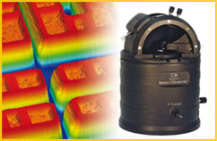
We will be exhibiting at the European Conference on Surface Science, ECOSS August 26-29 and look forward to meeting you at our booth no. 2 for free image processing advice and a SPIP demo. Feel free to bring your own surface image data from your research on a memory stick and our image processing experts will be pleased to give you detailed advice on how to process your own data.
Category Archives: News
Release: SPIP 6.7!
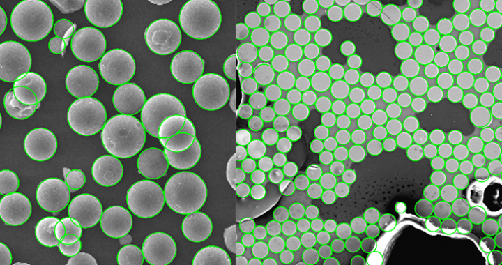
A Giant Leap for Particle Analysis!
With the new and improved detection and splitting options SPIP™ version 6.7 has taken a giant leap towards easy and robust particle analysis in SPM and SEM images.
New features include:
- New Circle detection option in Particle Analysis
- Improvement of watershed detection algorithms
- Automatic particle splitting functions
- Texture analysis for SEM and other non-height images
- Improved XY scaling tool
- New Particle & Pore Analysis Breadth parameters
- Save and load Measure Shapes
- Automatic outlier masking in Plane Correction
Learn more by reading the SPIP 6.7 leaflet:


Download SPIP
How to process information from Scanning Probe Microscopy
Scanning Probe Microscopy
Image Metrology's founder, Dr. Jan F. Jørgensen recently gave an interview discussing the field of Scanning Probe Microscopy, which below is re-produced for the knowledge of SPIP™ users.
The SPM Technique
 Scanning Probe Microscopy or SPM, is a technique that uses a very sharp probe to scan over a surface in a raster pattern. When the probe is within atomic distance of the surface an AFM (Atomic Force Microscopy) probe can sense the repulsive and attractive forces from the surface. The height of the probe is controlled such that the force is kept constant meaning that also the distance to the surface is kept constant. Therefore, a topographic landscape image can be produced by recording the z position of the probe for the x, y positions.
Effectively the AFM probe traces over the surface of a substrate and records the surface topography as it does so.
Scanning Tunneling Microscopy
STM (Scanning Tunneling Microscopy) works in a similar manner to AFM but uses a different sensing method. In STM there is a bias voltage set between the probe and the surface and when in atomic distance to the surface a tunneling current can be measured by the probe.
Because both of the techniques involve scanning very close to the surface it is possible to obtain images with atomic resolution.
The SPM Advantages
 The big advantage of SPM techniques compared to optical techniques is the ability to obtain height information and the unique capability of obtaining images at atomic resolution. SPM allows a lot of geometrical information to be extracted at a very detailed level.
To obtain geometrically correct images it is crucial that the movement of the probe relative to the surface can be controlled better than the desired resolution, which is a big challenge. It is almost impossible to create images where the pixels are acquired equidistantly and where there is no coupling between the axes. Even in the most perfect instrument problems with environmental noise, vibration and temperature changes will lead to imperfect images.
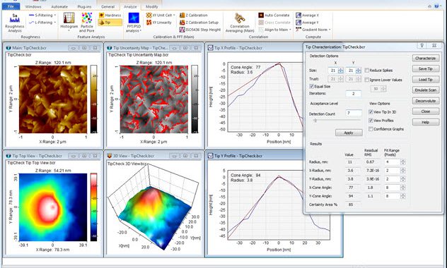
In SPIP™ we have implemented several methods to characterize imperfections and correct for them which allows extremely accurate measurements to be performed.
The new addition in SPIP 6.6.5: Nano-Observer file formats
In SPIP™ version 6.6.5 the file format of the CS Instruments’ Nano-Observer AFM has been implemented for images, force curves including flex grids, and force volume images (step grids).
Read more about the instrument here: http://www.csinstruments.eu/our-products/nano-observer-afm-microscope/
Join us at MRS Fall Meeting & Exhibit in Boston
We will be exhibiting at the 2016 MRS Fall Meeting in Boston on November 29-December 1., and look forward to meeting you at our booth no. 1100 for free image processing advice and a SPIP demo.
Feel free to bring your own image data on a memory stick if you want image processing experts to give you detailed advice on how to process your own data.
Contact us for information on how to receive your complimentary badge to the exhibition!
Nanosurf and Image Metrology renew OEM agreement
Nanosurf now offers SPIP™ as a standard component in their C3000 Advanced Spectroscopy Option, and as an optional component in their entire product range.
Founded in 1997, Nanosurf is a Swiss based high-tech company providing scanning probe microscopes to customers around the globe. The product range starts with very compact instruments, followed by state-of-the-art research systems, all the way up to fully customized and comprehensive solutions. Nanosurf is valued for their innovative approach, the modularity, and the ease of use of their products by its large customer base in research, industry and teaching.
Contact:
Nanosurf AG
Gräubernstrasse 12-14
4410 Liestal
Switzerland
Tel.: +41 61 927 47 47
Web: www.nanosurf.com
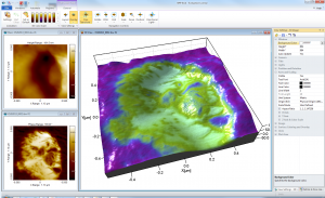
SPIP™ 6.6 featuring the new improved ImageMet Explorer™
Image Metrology is proud to announce the release of SPIP™ 6.6 featuring the new improved ImageMet Explorer™ with more speed and efficiency for searching, sorting and exploring files.